M A T E R I A L S
RESEARCHERS HARVEST
2-D MATERIALS, CLOSER
TO COMMERCIALISATION
Since the 2003 discovery of the singleatom
Protecting Marine Craft in New Zealand and the world for 30 years
Protecting Marine Craft in New Zealand and the world for 30 years
Superior Corrosion Prevention in New Zealand and the world for 30 years
Clear Protective Coating
Preserves both Metal and Painted
Surfaces
Highly Corrosion Resistant
Highly Cleansable Surface
Restores Paint Appearance
Long Lasting Protection
www.nyalic.co.nz
0800 692 542
Text 0274 351 069
✉ sales@nyalic.co.nz
Protecting Marine Craft in New Zealand and the world for 30 years
SuperioCr leCaor Prrrootescitoiven C Poarteinvge
ntion in New Zealand and the world for 30 years
Clear Hard Protective Coating
Highly Corrosion Resistant in
Aggressive Environments
Ideal for Circuit Boards and
Electrical Connections
Restores Paint Appearance
Long Lasting Protection
www.nyalic.co.nz
0800 692 542
Text 0274 351 069
✉ sales@nyalic.co.nz
Preserves both Metal and Painted
Surfaces
Highly Corrosion Resistant
Highly Cleansable Surface
Restores Paint Appearance
Long Lasting Protection
www.nyalic.co.nz
0800 692 542
Text 0274 351 069
✉ sales@nyalic.co.nz
Superior Corrosion Prevention in New Zealand and the world for 30 years REN152
Clear Hard Protective Coating
Highly Corrosion Resistant in
Aggressive Environments
www.nyalic.co.nz
Clear Protective Coating
Preserves both Metal and Painted
Surfaces
Highly Corrosion Resistant
Highly Cleansable Surface
Restores Paint Appearance
Long Lasting Protection
www.nyalic.co.nz
0800 692 542
Text 0274 351 069
✉ sales@nyalic.co.nz
Clear Hard Protective Coating
Highly Corrosion Resistant in
Aggressive Environments
Ideal for Circuit Boards and
Electrical Connections
Restores Paint Appearance
Long Lasting Protection
www.nyalic.co.nz
0800 692 542
Text 0274 351 069
✉ sales@nyalic.co.nz
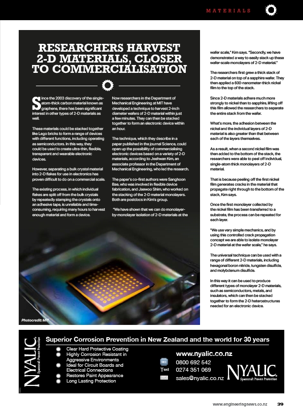
Photocredit: MIT
thick carbon material known as
graphene, there has been significant
interest in other types of 2-D materials as
well.
These materials could be stacked together
like Lego bricks to form a range of devices
with different functions, including operating
as semiconductors. In this way, they
could be used to create ultra-thin, flexible,
transparent and wearable electronic
devices.
However, separating a bulk crystal material
into 2-D flakes for use in electronics has
proven difficult to do on a commercial scale.
The existing process, in which individual
flakes are split off from the bulk crystals
by repeatedly stamping the crystals onto
an adhesive tape, is unreliable and timeconsuming,
requiring many hours to harvest
enough material and form a device.
Now researchers in the Department of
Mechanical Engineering at MIT have
developed a technique to harvest 2-inch
diameter wafers of 2-D material within just
a few minutes. They can then be stacked
together to form an electronic device within
an hour.
The technique, which they describe in a
paper published in the journal Science, could
open up the possibility of commercialising
electronic devices based on a variety of 2-D
materials, according to Jeehwan Kim, an
associate professor in the Department of
Mechanical Engineering, who led the research.
The paper’s co-first authors were Sanghoon
Bae, who was involved in flexible device
fabrication, and Jaewoo Shim, who worked on
the stacking of the 2-D material monolayers.
Both are postdocs in Kim’s group.
“We have shown that we can do monolayerby
monolayer isolation of 2-D materials at the
wafer scale,” Kim says. “Secondly, we have
demonstrated a way to easily stack up these
wafer-scale monolayers of 2-D material.”
The researchers first grew a thick stack of
2-D material on top of a sapphire wafer. They
then applied a 600-nanometer-thick nickel
film to the top of the stack.
Since 2-D materials adhere much more
strongly to nickel than to sapphire, lifting off
this film allowed the researchers to separate
the entire stack from the wafer.
What’s more, the adhesion between the
nickel and the individual layers of 2-D
material is also greater than that between
each of the layers themselves.
As a result, when a second nickel film was
then added to the bottom of the stack, the
researchers were able to peel off individual,
single-atom thick monolayers of 2-D
material.
That is because peeling off the first nickel
film generates cracks in the material that
propagate right through to the bottom of the
stack, Kim says.
Once the first monolayer collected by
the nickel film has been transferred to a
substrate, the process can be repeated for
each layer.
“We use very simple mechanics, and by
using this controlled crack propagation
concept we are able to isolate monolayer
2-D material at the wafer scale,” he says.
The universal technique can be used with a
range of different 2-D materials, including
hexagonal boron nitride, tungsten disulfide,
and molybdenum disulfide.
In this way it can be used to produce
different types of monolayer 2-D materials,
such as semiconductors, metals, and
insulators, which can then be stacked
together to form the 2-D heterostructures
needed for an electronic device.
www.engineeringnews.co.nz 39
/www.nyalic.co.nz
/www.nyalic.co.nz
/www.nyalic.co.nz
/www.nyalic.co.nz
/www.nyalic.co.nz
/www.nyalic.co.nz
/www.engineeringnews.co.nz
link
link
link
link
link